Ph.D.

Short Bio
Kahraman Keskinbora is a cross-disciplinary materials scientist with a Ph.D. in chemistry, an M.Sc. in nanotechnology, and a bachelor's degree in materials science and engineering. He works on nano-engineering of optical devices, micro/nano-fabrication, and X-ray microscopy. Since November 2020, he is working at MIT as a DFG Research Fellow. When he is not working in the lab, in a meeting, or glued to a screen, he is most likely to be traveling. His wavefunction extends over the Atlantic and he can be found on either side of the Pond at any given time. If you would like to learn more, read here.

Selected Publications
Part of my full publication list.

Bayesian Machine Learning for Efficient Minimization of Defects in ALD Passivation Layers
Gül Dogan,* Sinan O Demir, Rico Gutzler, Herbert Gruhn, Cem B Dayan, Umut T Sanli, Christian Silber, Utku Culha,* Metin Sitti, Gisela Schütz, Corinne Grévent, Kahraman Keskinbora*
November 4, 2021
Machine learning optimization meets materials science. Read the paper!

November 15, 2021
When you protect copper with a ceramic thin film you also electrically isolate it. How would you then electrically interface the underlying copper thin film? Here is how...
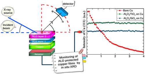
In Situ X-ray Diffraction and Spectro-Microscopic Study of ALD Protected Copper Films
Gül Dogan,* Umut T Sanli, Kersten Hahn, Lutz Müller, Herbert Gruhn, Christian Silber, Gisela Schütz, Corinne Grevent,* Kahraman Keskinbora*
June 6, 2020
An inquiry into the protective properties of ALD thin film stacks at high temperatures and pitfalls.

2019, SPIE Spotlights
Published online by SPIE Spotlights, this e-book is an introductory tutorial for master's and Ph.D. students who are starting to use the FIB/SEM instruments for prototyping micro- and nano-optics.

3D Nanoprinted Plastic Kinoform X-ray Optics
U. T. Sanli, H. Ceylan,* I. Bykova, M. Weigand, M. Sitti, G. Schütz, K. Keskinbora*
2018, Advanced Materials
In this work, we show 3D nano-printing of kinoform X-ray lenses using two-photon polymerization. The lenses were tested at soft X-ray energies showed a superb performance.

3D Nanofabrication of High-Resolution Multilayer Fresnel Zone Plates
U. T. Sanli,* C. Jiao, M. Baluktsian, C. Grévent, K. Hahn, Y. Wang, V. Srot, G. Richter, I. Bykova, M. Weigand, G. Schütz, K. Keskinbora*
2018, Advanced Science
This substantive work lead by my group appeared in the journal Advanced Science, and the journal selected our artwork as one of the covers of the issue. In the paper, Umut fabricated first ML-FZPs using ALD that can image 15-nm structures in a test target. We characterized the multilayers extensively and showed that its interfaces exhibit excellent structural sharpness and are chemically abrupt.

High-throughput synthesis of modified Fresnel zone plate arrays via ion beam lithography
K. Keskinbora,* U. T. Sanli, M. Baluktsian,
C. Grévent, M. Weigand, G. Schütz
2018, BJNANO
In this work, I applied the direct-write IBL to further decrease the outermost zone width of FZP structures to 30 nm while decreasing the fabrication time to below 10 minutes. Then, the IBL method was applied to fabricate an array of high-resolution FZPs. Each of the FZPs in this array can resolve 20-nm wide features.

Single‐Step 3D Nanofabrication of Kinoform Optics via Gray‐Scale Focused Ion Beam Lithography for Efficient X‐Ray Focusing
K. Keskinbora, C. Grévent, M.Hirscher, M. Weigand, G. Schütz
2014, Advanced Optical Materials
I spent a significant part of my Ph.D. developing a gray-scale direct-write IBL protocol for fabricating kinoform X-ray lenses in hard materials, which appeared in the frontispiece of the journal Advanced Optical Materials.

Rapid Prototyping of Fresnel Zone Plates via Direct Ga+ Ion Beam Lithography for High Resolution X-Ray Imaging
K Keskinbora, C Grévent, U Eigenthaler, M Weigand, G Schütz
2013, ACS Nano
In the work that appeared in ACS Nano, we described how direct-write ion beam lithography (IBL) to fabricate Fresnel Zone Plates (FZP) with outermost zone widths of 50 nm quickly. The fabrication part is followed by an extensive X-ray characterization.

Research Interests
An overview of the current research interests.
My research interests broadly revolve around nanotechnology and particularly nanofabrication of micro/nano-optics components. Design, materials selection, simulation, fabrication, and characterization are all parts of the research cycle we follow in my group. Here, I summarize the topics I have published so far.

Micro/Nano-Optics

Development of Nano-fabrication Routes

Soft-X-ray Spectro-Microscopy
Design, fabrication & testing of diffractive optics, and photonic devices.
Synergistic combination of Focused Ion Beam Lithography (FIB/IBL), Atomic Layer Deposition (ALD), and 3D Nano-printing.
Advanced imaging for testing of diffractive optics and investigation of complex materials.
2PP of a Fresnel Zone Plate
A femtosecond infrared laser scans the surface of a substrate, writing an FZP structure. The white light is the luminescence from the polymer upon laser irradiation. Structuring was done in Center for Nanoscale Science at Harvard.
Micrograph Gallery
I was lucky to work with amazing microscopes, and over the years I gathered many interesting images. Here are some of those images relating to both my research and outreach activities.